


Engineers produce smallest 3-D transistor yet
10. 12. 2018 | MIT | www.mit.edu
Researchers from MIT and the University of Colorado have fabricated a 3-D transistor that’s less than half the size of today’s smallest commercial models. To do so, they developed a novel microfabrication technique that modifies semiconductor material atom by atom.
The inspiration behind the work was to keep up with Moore’s Law, an observation made in the 1960s that the number of transistors on an integrated circuit doubles about every two years. To adhere to this “golden rule” of electronics, researchers are constantly finding ways to cram as many transistors as possible onto microchips. The newest trend is 3-D transistors that stand vertically, like fins, and measure about 7 nanometers across — tens of thousands of times thinner than a human hair. Tens of billions of these transistors can fit on a single microchip, which is about the size of a fingernail.
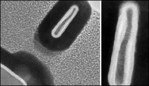
As described in a paper presented at this week’s IEEE International Electron Devices Meeting, the researchers modified a recently invented chemical-etching technique, called thermal atomic level etching (thermal ALE), to enable precision modification of semiconductor materials at the atomic level. Using that technique, the researchers fabricated 3-D transistors that are as narrow as 2.5 nanometers and more efficient than their commercial counterparts.
Read more at MIT
Image Credit: MIT
-jk-