


New stamping technique creates functional features at nanoscale dimensions
9. 12. 2016 | MIT | news.mit.edu
Engineers at MIT have invented a fast, precise printing process and created a stamp made from forests of carbon nanotubes that is able to print electronic inks onto rigid and flexible surfaces.
Team’s stamping process should be able to print transistors small enough to control individual pixels in high-resolution displays and touchscreens. The new printing technique may also offer a relatively cheap, fast way to manufacture electronic surfaces for as-yet-unknown applications.
There have been other attempts in recent years to print electronic surfaces using inkjet printing and rubber stamping techniques, but with fuzzy results. Because such techniques are difficult to control at very small scales, they tend to produce “coffee ring” patterns where ink spills over the borders, or uneven prints that can lead to incomplete circuits.
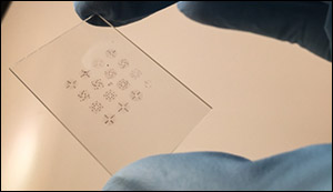
To make their stamps, the researchers used the group’s previously developed techniques to grow the carbon nanotubes on a surface of silicon in various patterns, including honeycomb-like hexagons and flower-shaped designs. They coated the nanotubes with a thin polymer layer to ensure the ink would penetrate throughout the nanotube forest and the nanotubes would not shrink after the ink was stamped. Then they infused the stamp with a small volume of electronic ink containing nanoparticles such as silver, zinc oxide, or semiconductor quantum dots.
Read more at MIT
Image Credit: MIT
-jk-